
High-density interconnection (HDI) PCB technology is advancing to enable increased miniaturization and functionality of products such as smartphones, tablet computers and wearable devices. This dictates continual reduction in feature size for conductor line width and spacing, micro-via pad diameter and pitch, and conductor and insulating layer thickness to accommodate more components and layers without increasing size, weight or volume of the PCB assembly. Furthermore, as wireless data transmission bandwidth and processing speed increase, electrical performance of the PCBs becomes ever more critical.
Just as the IC industry met serious roadblocks in feature scalability to keep pace with Moore’s law of doubling performance improvement, so the PCB industry now faces challenges in basic process capability and material properties to continue delivering improvements in interconnection density and electrical performance on their forecast trajectories. Even in the state-of the-art process node for all-layer-via (ALV) HDI design, limitations in process scalability and escalating factory cost raise questions about diminishing returns in packaging density and performance.
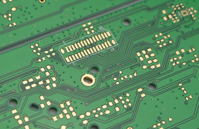 In particular, the industry faces significant challenges increasing PCB layer count and reducing thickness as individual insulation layers cross the 50 micron threshold, where degradation of dimensional stability and electrical performance (particularly signal impedance and resistance to leakage) accelerate, and increasing signal routing density below the 40 micron line width threshold where conventional subtractive technology fails and additive technology remains too costly and small in production scale to be a practical alternative.
While the increased use of sophisticated and adaptable automation such as laser direct imaging (LDI), sub 100 micron laser vias (LDD) and increased use of vision technology offer some improvements, escalating cost and hard limits in material performance suggest we need to focus on the fundamentals to make the system more robust, capable and affordable.
This paper will describe the recent challenges and developments in manufacturing ALV HDI technology to meet the needs for high volume, robust, reliable, and cost competitive solutions for electronic packaging.
Introduction
As the popularity of social media surges, increasingly communication is done through smart phones or tablets. Social media is now also a crucial part of any successful businesses marketing plan. It offers us a platform to interact with existing and potential customers and can often provide us with feedback and new ideas. That means the amount of data transferred has increased considerably in recent years and will continue. Subsequent increases in functionality, together with reduction in component size, have been the main drivers for PCB development. Semiconductor technology progresses at an almost exponential rate, typically doubling in functionality every couple of years and is expected to continue at this pace for several years to come.
When comparing typical rigid PCB structure used for the first mobile phones with current state of the art PCBs for smart phones, one can see tremendous differences. It can be said that miniaturization has been the predominant trend over the years. While the external dimensions of phones have not greatly changed, component and PCB size shrink to accommodate greater functionality has been remarkable; in a typical smart phone or tablet, a majority of space is occupied by displays and batteries as the remaining electronics have been downsized and integrated into small, compartmentalized spaces.