
Purpose of PCB Surface Finish
*Provides a solderable surface for Component assembly.
*Protect Copper Surface from Oxidation.
*Provide a surface appropriate for wear related parts.
High Performance Surface Finish
*Mixed Technology Board Designs
*Solderable,SMT and Thru-hole
*Wire Bondable
*Contact Resistance
*Co-Planar Surfaces
*Compatability with variety of fluxes & paste
*Cost effective
*Environment
Available Surface Finishes
*Electroless Nickle-Immersion Gold
*Immersion Silver
*Hot Air Solder Level
*Organic Solderability Preservative
*Electrolyte Nickel – Hard Gold
*Electrolyte Nickel – Soft Gold
Surface Finish Details
*Electroless Nickel-Immersion Gold (ENIG)
A two layer, gold over nickel, metallic surface finish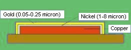
plated onto the copper base by means of a
chemical decomposition process.
Advantage: Disadvantage:
| *Typical Thickness: 3-8 uin gold over 150-250 | *Narrow process window |
| uin nickel | *Higher cost than HASL(1.5 to 2.0 times) |
| *Excellent Corrosion resistance | *Back pads: brittle solder joints |
| *Good for aluminium wire bonding | *Fatigue failures on large BGA packages |
| *Excellent flatness for fine-pitch technology | *Skip plate |
| *Excellent Solderability | *Extraneous nickel plating |
| *Excellent shelf life(12 mo) | *Solder mask capability with the nickel bath |
| *Good surface contrast | |
| *Good contact resistance | |
| *High Aspect Ratio Capability |